An all-in-one business management solution for all your business needs!
Book a free demo to know more!
-
Built to scale with your business.
-
AI-powered solution to automate workflow.
-
Cost-effective for growing businesses.


An all-in-one business management solution for all your business needs!
Book a free demo to know more!

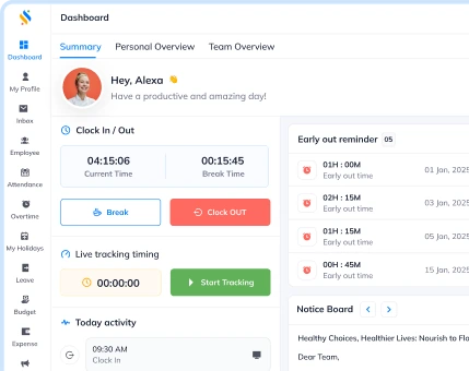
Your Partner in the entire Employee Life Cycle
From recruitment to retirement manage every stage of employee lifecycle with ease.
Your Partner in the entire Employee Life Cycle
From recruitment to retirement manage every stage of employee lifecycle with ease.